Reliable mmWave On-Wafer Measurement from Lab to Factory Floor
Members can download this article in PDF format.
What you’ll learn:
- Why on-wafer measurement is complicated at mmWave frequencies.
- How industry can benefit through knowledge transfer from metrology labs.
On-wafer calibration and measurement are underpinning technologies for the development of millimeter-wave (mmWave) integrated planar circuits, which have found homes in a large variety of applications. Prominent examples include wireless backhaul links for 5G mobile networks, automotive radar sensors, space-deployed radiometers for Earth remote sensing, radio astronomy, and more. Accurate on-wafer measurement is critical to the production of high-quality and assured integrated circuits for the above-mentioned applications.
S-parameters are fundamental electrical quantities for the characterization of integrated circuits (ICs). Measurement equipment such as probes working at frequencies up to 1.1 THz are commercially available. However, for a long time, no traceability has been available for on-wafer, S-parameter measurements beyond 110 GHz.
Many factors can significantly impact on-wafer measurement results at mmWave frequencies, including (but not limited to):
- The choice of calibration methods and reference planes
- Parasitic circuit elements associated with the interconnection between the probe and contact pads
- The test environment (e.g., metallic or ceramic wafer chuck)
- Coupling between adjacent neighboring structures on the same wafer
- Crosstalk between probes
- Propagation of unwanted modes, particularly for coplanar-waveguide (CPW) structures
- Damage/wear and tear of probes or calibration standards
Not considering these factors can often lead to inaccurate or inconsistent measurement results.
Ample efforts have been devoted to tackling these challenges and establishing traceability for S-parameter measurements up to THz frequencies, particularly by metrology laboratories. For example, two large-scale European projects, PlanarCal (2015-2018)1 and TEMMT (2019-2022),2 include work packages dedicated to these challenges. PlanarCal also developed a Best Practice Guide (BPG)3 on how to perform precise on-wafer S-parameter measurements using a VNA.
On an international level, the IEEE Standards Working Group P2822 was launched in 2021 to foster advances in the standardization of on-wafer measurements. This working group aims at developing recommended practices for performing accurate on-wafer calibrations, de-embedding, and measurements up to THz frequencies. National Physical Library (NPL) is actively involved in both the PlanarCal and TEMMT projects as well as the P2822 working group. However, all of these activities are aimed primarily at top-tier metrology laboratories rather than more general end-users working in the industry.
To facilitate the knowledge transfer from metrology laboratories to industrial end-users, NPL has been working with Filtronic Broadband on another European project: PlanarMeT. Filtronic designs and manufactures a broad range of microwave and mmWave modules for the point-to-point mobile backhaul market. On-wafer S-parameter measurements of integrated planar circuits, e.g. amplifiers, are a key step in their research and development process, and hence the work is very relevant to Filtronic.
Activities undertaken as part of PlanarMeT include production of a user-friendly industrial guide aimed at the non-measurement specialist and suitable for implementation on an industrial factory floor; and a measurement comparison exercise between NPL and Filtronic by following the user guide to demonstrate good quality measurements. These activities are discussed below.
Introductory User Guide
The PlanarCal BPG is a lengthy document and contains some very complicated information that requires a high level of user expertise/knowledge. To complement this BPG, there’s the need for a user guide (based on less complicated, practical, methods) that’s a concise document aimed at the non-measurement specialist and suitable for implementation on an industrial factory floor (rather than a top-tier precision metrology laboratory).
NPL and Filtronic addressed that issue by publishing a simple introductory user guide with open access.4 This Introductory Guide tutors end users on implementing straightforward methods to perform reliable on-wafer calibration and measurement at mmWave frequencies. The guide describes the key considerations affecting the accuracy of measurements, including experimental setup, choice of calibration methods, testing environment, crosstalk/isolation between probes, measurement verification, and design considerations for calibration kits. More details can be found in Reference 4.
Measurement Comparison
Confidence in measurement results can often be achieved by demonstrating good agreement between measurements made by different institutes, particularly a reference laboratory such as a metrology laboratory. NPL and Filtronic participated in a measurement comparison at D-band (110-170 GHz) by following the user guide.
CS-15, the commercially available Impedance Standard Substrate (ISS) manufactured by GGB Industries and designed for use above 110 GHz, was used to provide calibration standards and devices. Because the devices under test (DUTs) are on the same wafer as calibration standards, calibration was performed “on-wafer.”
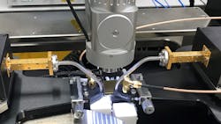
Figure 1 shows the measurement setup used at NPL, consisting of an MPI TS-150 manual probe station, Keysight's PNA-X N5247B VNA, a pair of D-band VDI mini frequency-extension modules, and a pair of D-band GSG probes with 100-µm pitch size. Calibrations and measurements were made using an IF bandwidth of 50 Hz and 601 frequency points. No averaging was utilized in the calibration or measurement.
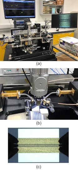
The ISS was placed on a ceramic chuck during all calibrations and measurements made in this study, to ensure consistency of the test environment. The ceramic chuck is helpful in terms of suppressing some spurious modes.
For the comparison, the participants used the line-reflect-reflect-match (LRRM) calibration method and the same set of calibration standards on CS-15—in other words, a 175-µm, 50-Ω coplanar-waveguide (CPW) line as the Line standard, a pair of open pads and shorting bars as the Reflect standards, and a pair of 50-Ω loads as the Match standard. The reference plane was set at the middle of the Line standard.
The study measured several devices (CPW lines with different lengths, offset short, offset open, and offset load) on the CS-15. A selection of measurement results of CPW lines with physical lengths of 1025 µm and 6600 µm is shown in Figure 2. After de-embedding, the effective lengths of these lines are 850 µm and 6425 µm.
As seen in Figure 2, the measured results from the two participants show very good agreement. The mean differences between the two participants’ values are around ≤ 0.002 µm for transmission responses and ≤ 0.023 µm for the reflection responses. The small difference is believed to be mainly attributed to alignment errors when positioning/re-positioning the probes on the calibration standards and/or DUTs. This can be improved by repeating the calibration and measurement or utilizing an automatic probe station.
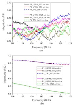
One participant also carried out through-reflect-line (TRL) calibration, the other popular calibration method utilized in the industry. The calibration used the same 175-µm line as the Thru standard, a pair of shorting bars as the Reflect standards, and a 355-µm line as the Line standard.
The difference in length between the Thru and Line standards, 180 µm, provides a phase delay of around 54°~83° across D-band. Again, the reference plane was set at the center of the 175-µm CPW line (i.e., the Thru standard). Figures 2a and 2b show the comparison of measured results between TRL and LRRM, which are in good agreement.
Conclusions
This article covers a knowledge-sharing activity between NPL and Filtronic related to on-wafer measurement. We've produced a concise User Guide to provide industry-level methods for validating planar calibrations and measurements at mmWave frequencies. The good agreement in the measurement comparison exercise shows that the guidance given in this user guide can help end-users achieve accurate and consistent results at these very high frequencies.
Acknowledgement
This work was supported by the European Metrology Programme for Innovation and Research (EMPIR) Project 19SIP02 “Knowledge transfer of planar calibration and measurement techniques at millimetre-wave frequencies.” The EMPIR Programme is co-financed by the participating states and from the European Union’s Horizon 2020 Research and Innovation Programme.
References
1. PlanarCal Project (2015-2018), European Metrology Programme for Innovation and Research (EMPIR): https://planarcal.ptb.de/.
2. TEMMT Project (2019-2022), EMPIR: http://projects.lne.eu/jrp-temmt/.
3. Uwe Arz, et al, “Best Practice Guide for Planar S-Parameter Measurements using Vector Network Analysers”, EMPIR 14IND02 PlanarCal, 2018. https://doi.org/10.7795/530.20190424B.
4. Xiaobang Shang, Nick Ridler, Jian Ding, Mike Geen, “Introductory Guide to Making Planar S-parameter Measurements at Millimetre-wave Wavelengths,” EMPIR 19SIP02 PlanarMeT, 2021. https://doi.org/10.47120/npl.9001.
About the Author
Xiaobang Shang
Senior Research Scientist, National Physical Laboratory (NPL)
Dr. Xiaobang Shang, who began working for NPL in 2017 as a senior research scientist, develops measurement techniques for mmWave and THz frequencies, particularly on-wafer measurements. His current research interests also include the characterization of dielectric materials and microwave technology for quantum applications.
